
BJT Vs FET
Almost in every electronic device today transistors are used. So, transistor is one of the very important and the basic component today. There are lots of transistors till date have been manufactured. So, what is exactly a transistor is?
From the name transistor we can infer,
Transistor = Transfer + Resistor
Hence it is a combination of Transfer of Resistance. It Transfers resistance from high to low. This is the important property which makes it very useful and the important and very necessary component in the electronic devices.
Transistor is a semi-conductor device which can both conduct as well as insulate accordingly. It is used to amplify current, voltage or power, it is also used for switching purposes. It actually controls the current flowing. Major two of the uses as mentioned are amplifying and switching. They are very small is size and are robust.
Before transistor were invented, vacuum tubes were widely used but as the tiny and the decisive was invented around 1950s and then advancement in it took place and they are widely the most and the important part in devices today. Smartphones, laptops, computers or any other electronic devices contains this part. The processor which is the heart of the computer also contains millions of the transistors. It is also an integral part of the integrated circuits.
Till date almost around sextillions of transistors are manufactured.
Types Of Transistors
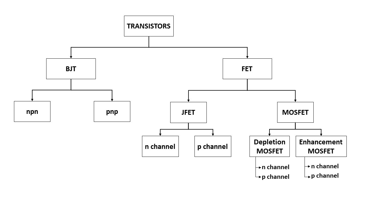
Classification of Transistors
Overview of BJT
BJT stands for Bipolar Junction Transistor.
From the name it says that bipolar means two types of charge carriers will be responsible for the flow of current. The majority and minority carriers both the electrons and the holes will be constituting the current. The transistor is made up from semi-conductor materials like silicon, germanium. Two pn junction diodes back-to-back on a silicon wafer gives a transistor.
It is a 3-terminal device.
The base, the collector and the emitter.
Emitter - as the name suggests it emits the majority charge carrier for the flow of current.
COllector - as the name suggests is collects the emitted majority charge carrier from the emitter and recombination takes place.
Base - This is less in width and lightly doped as it passes the carriers to the collector which are emitted by the emitter. This is kept so as it not allows most of the recombination to be done in the base.
Doping wise the emitter is doped the most, followed by the collector and then least doped is the base.
Width wise the base is least in width, intermediate is the emitter and then the collector is with maximum width.
These both is essential and important for the transistor, as the emitter emits the the majority charge carrier so it is highly doped and the collector is collecting the carriers so doped intermediately. As collector is meant for collecting the carriers, so it involves the dissipation of heat so the width is high of the collector. As the base is meant for the passing the carriers from emitter to the collector it is least doped and also the width of it is small.
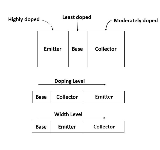
Dopping & Width levels of Base,collector and Emitter
Further the BJT is classified into two types i.e. npn type and pnp type.
In npn type the p is the base which is sandwiched between two n types which serve as the emitter and the collector. Similarly, in pnp type the n is the base which is sandwiched between two p types which serve as the emitter and the collector. If one type is understood properly then the other one is easy to understand as it is completely opposite to each other.
As the transistor can be used for switching and amplifying purposes, the proper biasing and making the Q point in the appropriate region is must.
There are three regions:
Saturation Region - The both collector-base and the emitter-base is forward biased.
Active Region - The collector-base is reverse biased and the emitter-bases is forward biased.
Cut-off RegionThe both collector-base and the emitter-base is reverse biased.
Breakdown Region - The region in which the transistor is beyond its limits.
For amplifying purposes, the transistor should operate in the active region and for the switching purposes, the transistor must be operated in the saturation and the cut-off region.
Also, there are different types of configuration for different amplification and different purposes.
Common Base Configuration: The input and the output are common to the base.
Common Emitter Configuration: The input and output are common to the emitter.
Common COllector Configuration: The input and output are common to the collector.
The different parameters related to the BJT are:
Input current Ib which is the base current
Output current Ic which is the collector current>
Vbe which is the voltage between base and the emitter
Vce which is the voltage between collector and the emitter and is the output voltage.
There are also many other parameters related to transistors like β, hfe and many more other, which are not being discussed here as are not required.
There are also many other parameters related to transistors like β, hfe and many more other, which are not being discussed here as are not required.
Ic = f(Ib)
Hence it is referred to as the current control device.
Along with these the input and the output characteristics of the transistor is also important and studied, which is a plot of input voltage Vs the input current and the output voltage Vs the output current respectively. This curves (plot) helps in determining the behavior and the characteristics exhibited by the transistor for various values of the current and voltage. From this the conductivity of the transistor can be determined.
Overview of FET:
FET stands for field effect transistors.
This are unipolar type which means that only either the electrons or the holes will be the carriers responsible for the flow of current. Hence unipolar only one of the of the charge carrier constitute the flow of the current. The field effect in the name has a meaning. It specifies that the electric field which is established due to the charge carriers will control the conduction path of the output circuit without the direct contact between the controlling and controlled quantities.
Mainly it is a 3-terminal device. Sometimes there are 4-terminals present.
The main 3 terminals are the gate, the drain and the source. The 4th which is present sometimes is the substrate of the body. Usually it is internally connected with the source making it 3-terminal device.
Source – as the name suggests it is the source for the electrons.
Drain – as the name suggests it is the sink for the electrons from the source.
Gate – It is the controlling type part between the source and the drain.
Substrate – the base layer of the transistor.
The FET are further classified as mentioned in JFETs i.e. Junction field effect transistors and MOSFETs i.e. Metal Oxide Semiconductor field effect transistors. Further classification in the former is n channel and the p channel. As FETs are unipolar so the there might be the n channel for the electrons as the charge carrier and p channel for the positive type charge carrier. Similarly, classification in the latter (MOSFET) is DMOSFET and EMOSFET which further for each category is n channel and p channel. The more detail about each type of FET will be not discussed here, it will be covered in separately section.
Also there exists the important parameters for the FETs,
The output current i.e. the drain current ID.
The input current i.e. the gate current IG which is zero for the proper working of the transistor and hence it has the high input impedance.
The input voltage i.e. the gate-source voltage VGS which controls the output current.
The output voltage i.e. the drain-source voltage VDS
There are also many more parameters related to the FETs like VP, IDSS , k and many more.
The output current is depended on the input voltage, i.e. the output current ID is the function of the input voltage VGS.
ID = f(VGS)
Hence the FETs are called as the voltage-controlled devices. One of the important differences between the BJT and FET.
In FET also there are three major regions:
Ohmic region - The region in which the transistor acts linearly.
Saturation Region - The region in which the output current obtained is constant.
Cut-off Region - The region in which the output current is zero.
Breakdown region - The region in which the transistor is beyond its limits
Here also there are the drain characteristics (output characteristics) and the transfer characteristics (input characteristics) which are very important in analysing the transistors and determining in which region do they operate and where is the Q point.
The Drain characteristics is a plot of the output voltage VDS Vs the output current i.e. the drain current ID. The Transfer characteristics is a plot of the input voltage VGS Vs the output current ID. These plots help in analysing the transistor.
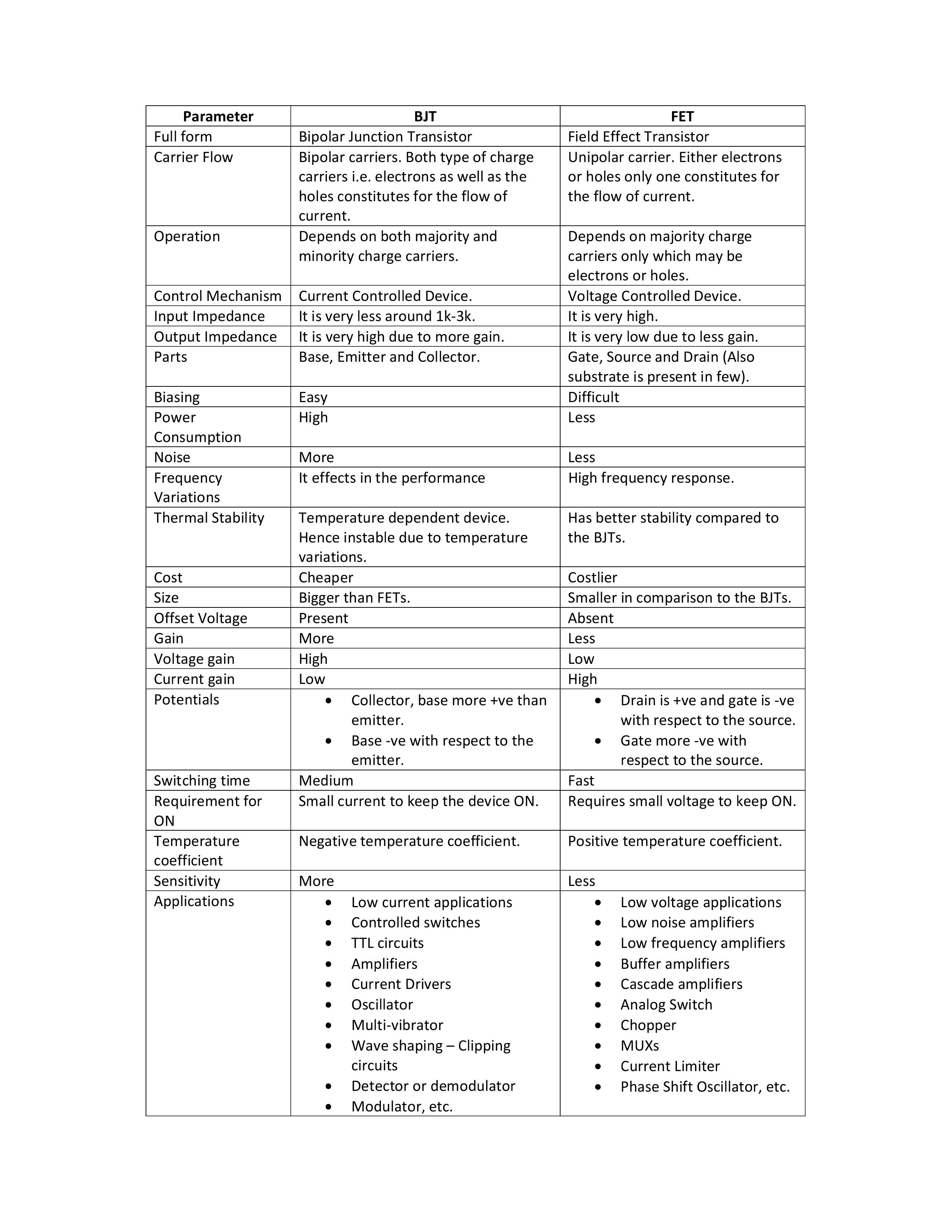
Difference between BJT and FET
Today MOSFETs are widely used and have overcome the BJTs in there usage due to there various advantages mentioned. BJTs initially were used everywhere and dominated but as the invention of FETs and then MOSFET took place and advancement in same made the FETs more in usage. Still BJTs are used at places where they are required and they do overcome the FETs in few cases. This what all makes BJT and FET different.
Discuss about post